I made a custom PCB to log data from different sensors to an SD card. This was partly motivated by wanting to track my RC plane’s flight path, but also as an exercise to expand my embedded systems engineering skills.
The hardware & firmware files are available on Github: https://github.com/benjohnemmett/Datalogger
Design
The main requirements for this project were:
- Run on a small rechargeable battery
- Read data from a GPS module
- Write location data to an SD card
- Fit in an RC plane (specifically the FT Tutor)
Extra nice-to-haves were:
- Read data from other I2C sensors
- Read data from other analog sensors
I decided to use what I already had for the main components:
- ATMega328P microcontroller
- BN-220 GPS Module + Antenna
- Lipo 2S 300 mAh with XT-30 connector
SD Card Compromise
This was my first time integrating an SD card with a microcontroller. I prototyped the design with some modules that handle the logic level conversion and provide breakout pins.
For interfacing with the SD card file system some research pointed me to the FAT FS library, which is a platform independent C-based library for reading/writing from/to a FAT filesystem. It was pretty easy to compile FAT FS with some test code, however when running the test code I constantly ran into read/write errors. I don’t have a debugger at this time to dig into the problem deeper so I decided to give the Arduino SD library a try instead and it worked great. So, this project is using Arduino for now, to get things off the ground. I’d like to return to FAT FS later and try to get it working.
Hardware Design
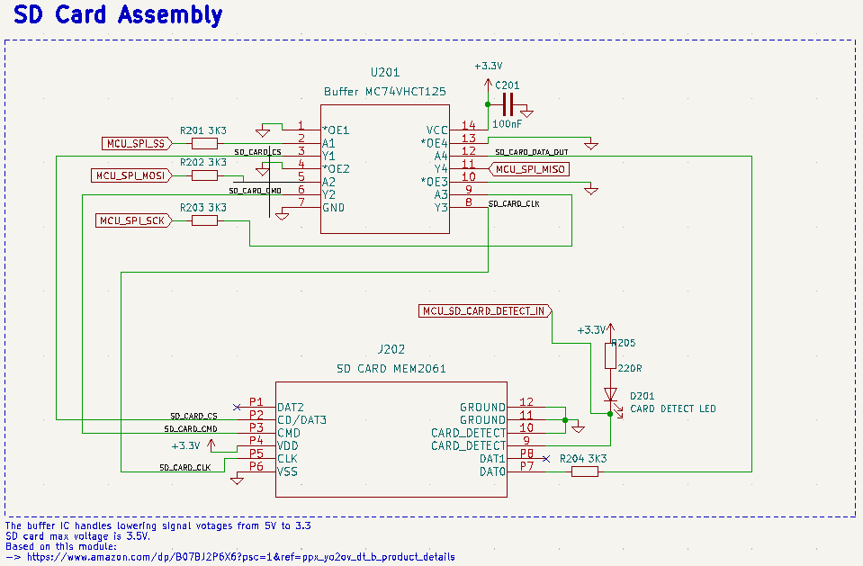
I based my project around an Arduino compatible ATMega328P, powered by a Lipo 2s-3s battery. The ATMega is running at 16MHz @ 5v. The SD card operates with a voltage range of 2.7v to 3.6v, so there are two separate power regulators for 5v & 3.3v.
The store listing for the SD card modules included a schematic which I used as a basis for my SD card assembly, including the MC74VHCT125 buffer IC to convert logic levels.
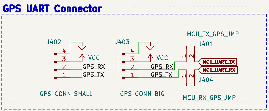
I added headers for my FTDI serial to USB converter. The GPS and FTDI both communicate over the only UART interface on the ATMega328P, so I added header pins to be able to disconnect the GPS from the UART pins.
The schematic also consisted of:
- Header pins for the SD card module used in testing
- 5 LED status lights
- 2 DIP Switches
- 3 I2C headers
- 4 Analog In (with Vcc & Gnd) headers
- Capacitor/Inductor filtering of analog Vcc (per Atmega328 datasheet recommendation)
PCB Layout
It took me several hours (over a few days) to turn this
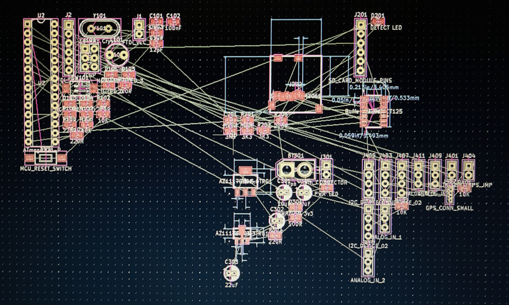
Into this…
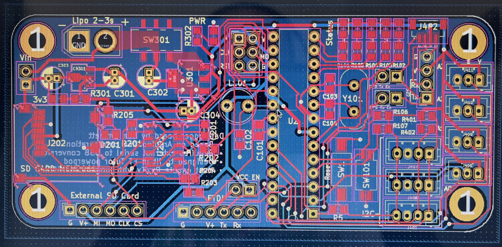
I used a 2-layer board with the backside mainly being a ground plane and the frontside used for routing most of the power & signals. Of course there is a lot going on here and I had to use the backside for signals and Vcc as well.
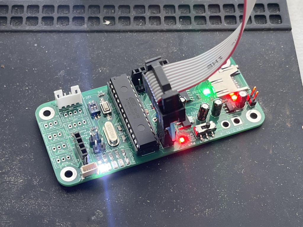
I ordered 10 boards + a solder mask from JLCPCB. They came after a couple weeks and look great.
Mistakes Were Made, Problems Were Resolved
Issue #1: Vcc/Ground Short
When bringing up the board I saw a huge current draw which indicated a short between Vcc & Ground. After poking around, I found that I had used the wrong package type in the 5v regulator.
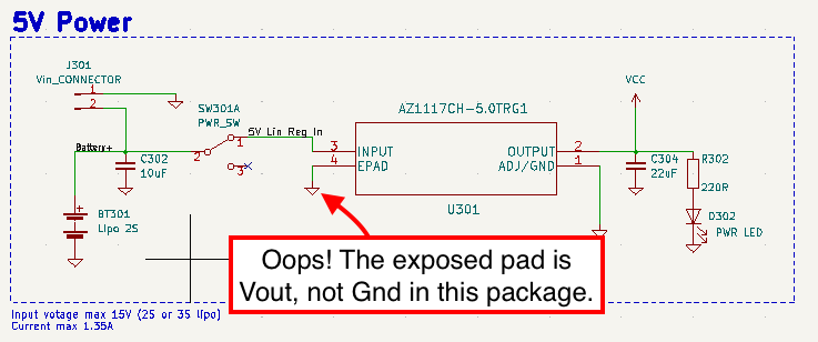
There is a package type with the exposed pad connected to ground, however I have the H package, not the H2.
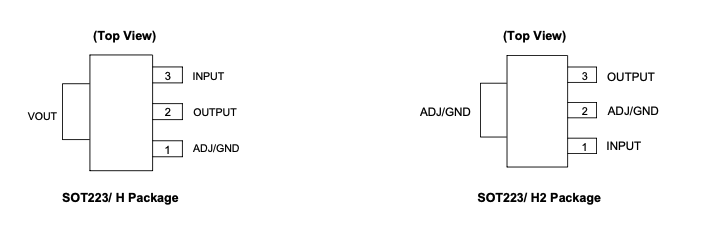
Lesson #1: Check IC package layout carefully.
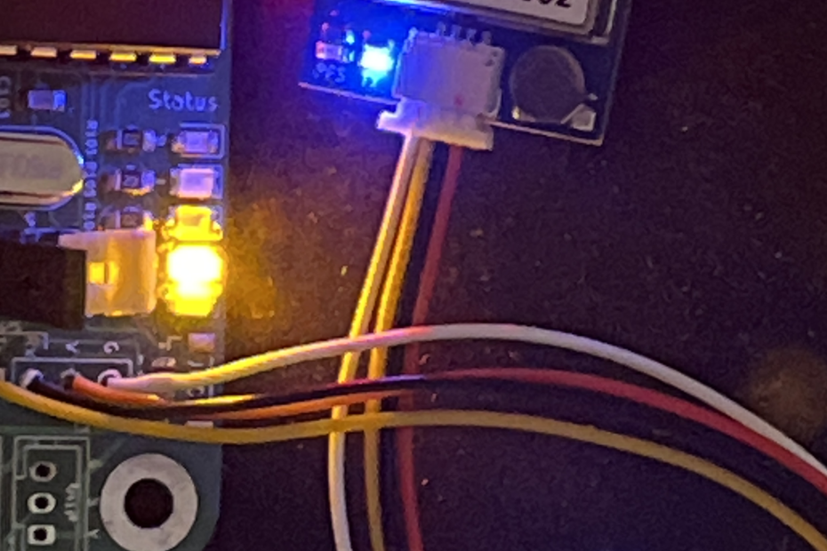
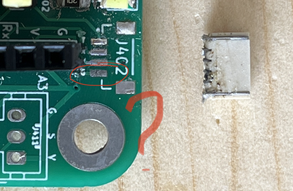
Issue #2: GPS Connector Order
I could not find a supplier with JST SH 4-pin connectors in stock so I ordered them from Amazon. I did not have them in hand while doing the layout, nor did I bother to go find a data sheet for them. They’re just simple connectors after all, what could go wrong? … Well somehow I put the connector pads in the reverse order from the cable supplied with the GPS module.
Another point that complicated the connector layout is that the cable that came with the GPS module does not have the same ordering on both ends. I only noticed this after I had finished all the PCB layout and was just about to order the boards. So I was feeling a bit rushed when I “fixed” the layout to another incorrect order.
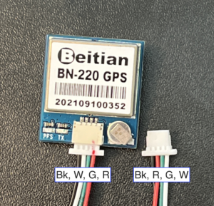
The solution to this is very simple. I made a custom connector with the wiring to match my connector layout. Still, there is a lesson here.
Lesson #2: Check the pin order on both ends of all connections
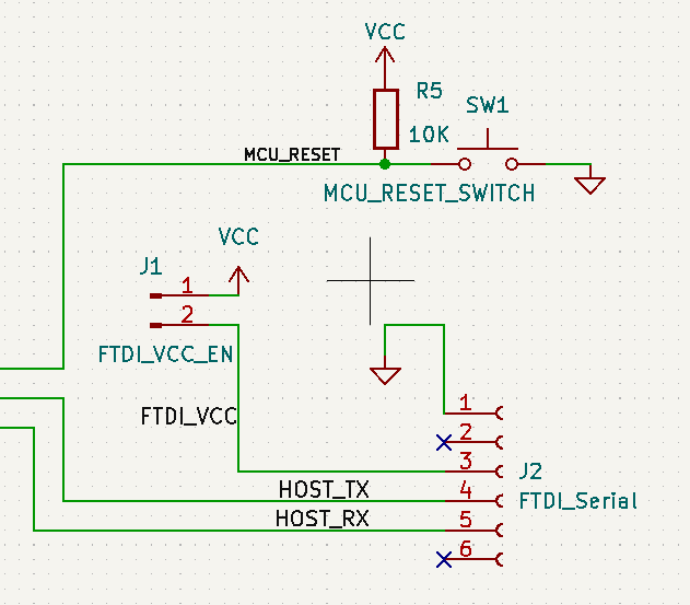
Issue #3: Arduino Programming
In order to program this with Arduino, I added FTDI headers. I made sure to use an ATMega328P that came preloaded with the Arduino bootloader. I gave it an external 16Mhz Crystal and 5v power, but I missed a critical feature. I did not coupling the reset pin to the DTR (Data Terminal Ready) pin of the FTDI adapter.
This problem was not hard to work around. The board can still be programmed using a USBAsp programmer using the Arduino IDE.
- In the Arduino IDE, set the following:
- Board -> Arduino Uno
- Port -> none (or set to the FTDI port if using it for serial monitor)
- Programmer -> USBAsp
Then flash the program with ⌘/Ctrl + Shift + U (Or Sketch -> Upload Using Programmer).
The FTDI adapter can still be used to capture print statements in the serial monitor, just not for flashing the program.
Lesson #3: Check the details of the design requirements
Issue #4: SD Card Detect
The SD card sockets came from Dig-Key, which generally provides a good data sheet for the products they carry, however this data sheet was not complete. When I saw that the footprint consists of two “Card Detect” pads I instantly assumed they were the two ends of a single pole single throw switch. However, that assumption was wrong. After powering up the board and seeing that the card detect light was constantly on I found the data sheet for a similar socket which showed how it actually works.
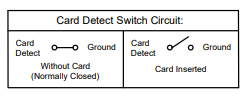
Both “Card Detect” pads (9 & 10 below) are actually shorted together and when no card is present, they are both shorted to ground. When a card is present they are both open and floating. In my poor design based on a bad assumption, I connected one pad to ground and the other to an LED light causing the light to be constantly on.
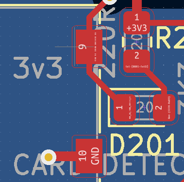
This issue also appears to have an easy fix, though I haven’t tried it yet. Cutting the trace from pad 10 to ground would leave pad 10 floating. Then pad 9 would connect the LED to ground when no card is inserted, and leave it floating with a card present. This would create an inverted card detect circuit (Light on == no card, light off = card present). I mainly wanted the card detect for the microcontroller, not the indicator LED. It is not currently used and I’m not sure I’ll bother to fix the issue at this point.
Still, lesson learned…
Lesson #4: The data sheet of a similar part is a better resource than a blind assumption
Issue #5: It’s just not working
Once the board was powered up the Arduino SD library call to SD.begin() would fail every time. It was as though the SD card connection was no good. I tried quite a few things to track down the issue including:
- Tested with SD Card module instead of on board SD card socket (still failed)
- Removed the Card detect light (who needs it anyway, it’s always on and sucking power for no reason)
- Removed SD card socket and resoldered
- Double checking the Chip Select pin was correct (It wasn’t but the issue persisted after setting it to pin 10 (PB2))
- Tested with Arduino example code (still failed)
- Removed ICSP programmer (just in case it was interfering with the SPI data transfer, still failed)
- Checked all connections with a multimeter (checked out, still failed)
- Added a bit more solder to each SD card socket pad + 3.3v buffer pin. (It works!)
Most of these things were done multiple times and it it’s hard to know which ones were helpful or not, though it appears that the main issue was a bad solder joint.
Lesson #5: When in doubt throw a bunch of troubleshooting techniques at the wall and see what sticks
Issue #6: Dead Pad
After some initial testing and collecting location data on the SD card, the GPS module suddenly stopped working. This had me stumped for a while longer, though it turned out that the ground pad under the JST connector was no longer connected to ground. There is no visible sign of break or tear and I’m not sure what happened.
The GPS module still worked when plugged into the extra 2.54 mm headers. Not wanting to send this up in an RC plane with jumper wires in a header socket that can easy pop out, I soldered the wired directly to the spot where the headers had been.
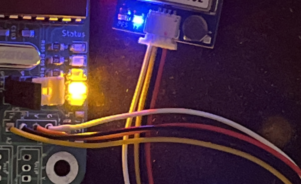
Hot glue has since been laid down to provide strain relief.
Lesson #6: The best laid plans still need backup plans
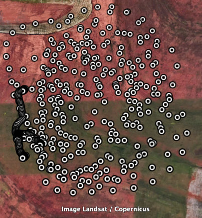
Field Testing
The real test was sending the data logger up in the an RC plane where I gathered a few minutes of GPS data at 1Hz. Here are the points scattered around incoherently on Google Earth Pro.
Conclusion
This project was a success on multiple levels. In the end, I have a lightweight GPS data logger to put on my plane. It has potential to log additional I2C & analog sensor data as well. The bigger success is that I finished a project that was beyond my skillset and learned quite a bit in the process.
What Do German GPS Systems Say When You Reach Your Destination?…Nein Miles Left To Destination